Prototyping and Testing for Driver Board Validation
Custom Development Journey (Part 2): Prototyping and Testing for Driver Board Validation
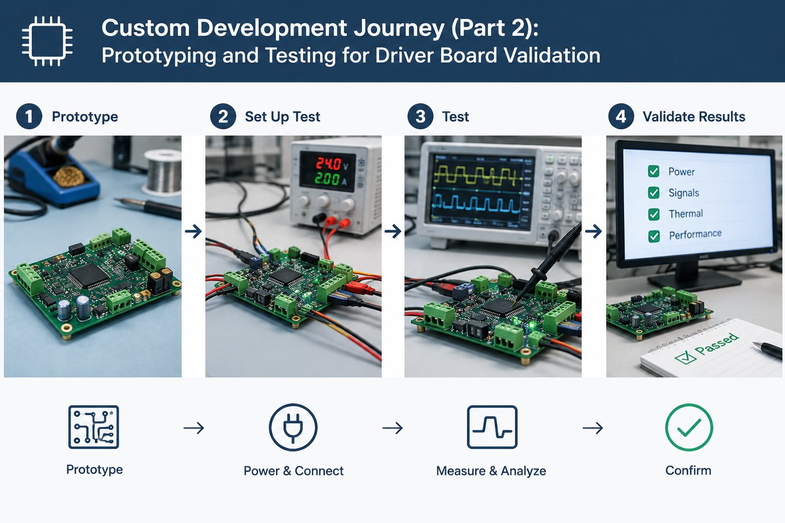
Getting the prototypes in hand is where validation actually starts: whether this driver board earns a spot in pilot production comes down to how systematic the testing has been. This article works through prototype verification in the order of “static inspection → functional testing → burn-in and temperature rise → EMC and safety compliance”. You get a ready-to-use test checklist and clear pass/fail criteria for each item.
Before Power-On: Static Checks and Staged Power-Up
Boards fresh from the assembler should never go straight onto power. First pass is visual inspection: look over the solder joints for cold joints, solder bridges, and solder balls, and confirm that polarized components (electrolytic capacitors, diodes, optocouplers, and IC orientation) are placed the right way round. Then check the board against the BOM and silkscreen finalized in the design review to confirm the key components match, especially the voltage ratings of the bus capacitors and power transistors. Catch this kind of wrong part now, while rework is still cheap.
Second pass is impedance checking. With a multimeter, measure the forward and reverse impedance from each power rail (power bus, 5V, 3.3V, and so on) to ground, then compare readings across several prototype boards. A rail that reads noticeably lower than its siblings usually points to a short circuit or a reversed component.
Third pass is staged power-up. The recommended sequence:
- Feed the logic section from an adjustable DC supply current-limited to 100–200mA, and watch each rail on an oscilloscope: you want stable voltage with no overshoot or ringing;
- Once the logic rails are stable, remove the current limit, bring up the rated bus voltage (the 24V or 48V setting, say), and observe the no-load quiescent current;
- Check the static levels of the enable and alarm outputs. Once those are confirmed correct, move on to functional testing.
Functional Testing: Work the Checklist and Log the Data
This is where every design commitment turns into measured data. Work through the order of power → interfaces → outputs → protection → communications, and for each item record the setpoint, the measured value, and the pass/fail call. That record is what makes the whole test traceable:
- Power and sequencing: voltage accuracy, ripple, and power-up/power-down sequencing of each rail;
- Control interfaces: pulse/direction/enable response and voltage-level compatibility; alarm output level and pulse width;
- Current and microstepping: measured accuracy of the set current, sinusoidal quality of the phase currents, and consistency between the two phases;
- Closed loop and fieldbus: encoder readback and lost-step correction; RS485/CANopen/EtherCAT message coverage, reconnection after cable breaks, and parameter retention through power-off;
- Protection functions: manually trigger overcurrent, overvoltage/undervoltage, over-temperature, and stall protection one by one, then verify thresholds, response times, and recovery behavior.
Current accuracy takes one simple calculation: I=V/R. With a 50mΩ sense resistor and an oscilloscope reading of 100mV peak, the peak current is 2.0A. Compare that against the value set from the host; if the error sits within the promised tolerance (commonly ±5% to ±10%), it passes.
| Test Item | Key Focus | Acceptance Criteria | Common Tools |
|---|---|---|---|
| Power rail quality | Voltage accuracy, ripple, and sequencing | Deviations within component specs and design commitments | Multimeter, oscilloscope |
| Phase current waveform | Sinusoidal shape, peak value, and symmetry | Both phases consistent, no obvious distortion or overshoot | Oscilloscope with current probe |
| Protection functions | Trip thresholds and recovery method | Trips as configured, recoverable, no false trips | Adjustable load, temperature chamber |
| Fieldbus communication | Message coverage and reconnection after link loss | Continuous operation without dropouts, errors under control | Host PC, bus analyzer |
Burn-In and Temperature Rise: Find the Weak Points Early
Early failures (cold joints, marginal parameters) mostly cluster within the first few dozen hours, so burn-in usually runs continuously for 24–72 hours at full load or with a periodically alternating load, with elevated temperature added when needed. Rule of thumb: electrolytic capacitor life roughly halves for every ~10°C rise in ambient temperature. Logging temperature curves during burn-in costs little and builds data for lifetime assessment down the road.
Before testing the board, do a thermal estimate so the thermal margin is known in advance: with a 48V bus and a stall phase current of 4A, conduction loss is roughly 2×I²×Rds(on), about 1.6W at 50mΩ, and switching losses come on top of that. With natural convection alone, the junction-to-ambient thermal resistance of a TO-220-type package is typically 40–65°C/W, so 1.6W already means more than 60°C of rise. At that point you’re into heavier copper pour, a heatsink, or a device with lower on-resistance.
For measured temperature rise, start with thermal imaging to scan the whole board for hot spots, then pin down the case temperatures of the power transistors, sense resistors, and inductors with thermocouples; measure the average winding temperature rise with the resistance method. As reference limits, windings in insulation classes A/E/B/F/H typically have resistance-method rise limits of 60/75/80/105/125K. For the power devices on the board, judge by junction temperature: designs usually require at least 20%–30% junction temperature margin at full load, and the measured values should corroborate the thermal estimates.
EMC and Safety Compliance: Don’t Leave Problems to the Certification Stage
The switching on a driver board is itself a source of interference. At the prototype stage, run a self-check with a spectrum analyzer and near-field probes, tracing noise sources and coupling paths along the chain of “power switches → gate-drive traces → interface cables”, with the focus on the conducted (150kHz–30MHz) and radiated (30MHz–1GHz) bands. Remediation then works through source → path → interface: adjust switching speed and snubber circuits, shrink the switching loop area, improve grounding, and add common-mode filtering and ferrite rings at the power and signal ports.
The heart of safety compliance is insulation and energy control. Take a high-voltage design with a rectified DC bus of about 310V: per the insulation coordination tables for Pollution Degree 2 and Material Group III, the creepage distance for basic insulation is about 3.2mm, and reinforced insulation needs double that (always defer to the standard’s tables here). Requirements for 24–48V low-voltage designs are relatively relaxed, but functional insulation, input fusing, and enclosure fire safety are still required (X-capacitor discharge resistors apply to AC-mains inputs only). The compliance workload differs greatly between the two approaches, so weigh it in at the solution design stage.
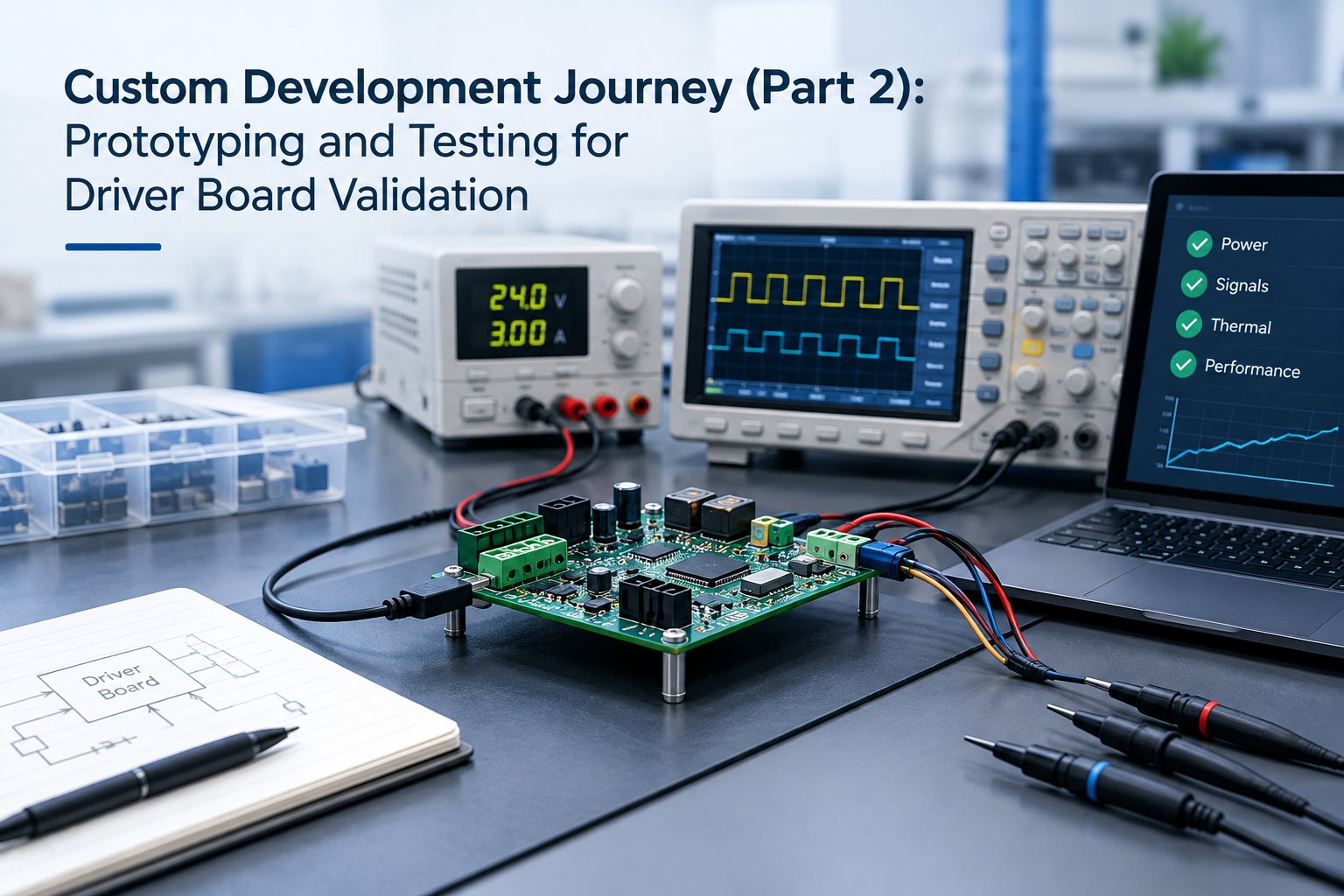
▲ Knowledge map of this article
For dielectric withstand (hipot) testing, run a baseline test at the prototype stage and routine tests in mass production: choose the test voltage and duration according to the working voltage level, verifying the insulation from the main circuit to ground and between the high- and low-voltage sections. A clean baseline test takes much of the risk out of certification later.
Working on a custom driver board? Have a look at HFY DRIVE’s custom driver board solutions for your next project.